Tuesday, June 23, 2009

How Do You Use The SMT Website?

Electronic information delivery — through digital magazines, e-newsletters, Websites, RSS feeds, etc. — is essential to the modern business world. Global and instant availability via the Internet has made information accessible, useful, and impactful in a way as momentous as the advent of the printing press. SMT is redesigning our Website, smtonline.com, to better fit you, our readers. While we engineer this Website, we’d like to hear what you want.

We’ve organized our technical features into focused categories, where you can find an article about lead-free rework easily, and click straight from that article into a section about cleaning residues from lead-free assemblies. All the while you’ll have recent news and product releases updated daily and accessible throughout the Website. The goal is to make information as easily accessed as if you had editors sitting with you, suggesting an article to meet your needs.

SMT usually polls its readers about industry challenges, such as lead-free, or business direction, such as capital equipment investments. Today, we want to know how you use the Internet, and what you’d like to see on the new-and-improved smtonline.com. Click through to our survey, “What do you want more of on smtonline.com?” and let us know what you want. We’ll keep the survey open through to the launch date of the new SMT Website, incorporating as many of your suggestions as possible. Got an idea for the site that isn’t on the survey? Leave a comment here on the blog.

Meredith Courtemanche, managing editor

Tuesday, June 16, 2009

Cleaning Electronics Assemblies — How Far We’ve Come

In the May/June issue of SMT, I wrote a round up of comments on cleaning, but there just wasn’t enough room to include everything. And, in the desire to say it all, here are some important facts that weren’t covered in the article, “Cleaning Equipment and Materials Trends.” The history of SMT cleaning helps us understand modern cleaning technologies as well as what’s in the research pipeline.

We have come a long way from the 1985 Montreal Protocol to methods of improved cleaning that have less of an environmental impact. The cleaning trend since the 1980s has shifted from a no-clean process to an emphasis on cleaning, especially with lead-free pastes/fluxes and higher processing temperatures. Defluxing used to be reserved for military and medical manufacturers, and now even boards for commercial products require defluxing.

Modern cleaning equipment generally performs faster with less power, less water, and fewer chemical additions. Strict quality control tolerances and traceability via statistical process control (SPC) data recording are expected from the latest equipment. As operators place assemblies into defluxing equipment, barcode information is immediately scanned, and one more step in the assembly process is recorded.

Technology has moved upstream. Conventional SMT assemblies use low-residue, no-clean soldering practices. Modern challenges for PCB cleaning hinge on high-density miniaturized assemblies with lower standoff heights and decreased area-array pitches. I also discussed the training and education necessary for the modern cleaning processes in "Spring Cleaning: Facility Implementation Is Key.”

There are a variety of ways to clean: aqueous, semi-aqueous, plasma-based, sonic-based, or through specialty chemical formulations that fit the particular paste/flux/component combination.

We didn’t talk enough about the amazing research work being done in this field. Ning-Cheng Lee is one of the researchers working on the best cleaning method to fit each lead-free material/flux application. He has tested many methods and materials and has come up with a best-fit system for many materials and equipment. His research will be presented at SMTAI this year in San Diego.

The High Performance Electronics Cleaning and Coating Symposium is a premier conference focused soley on cleaning to be held September 30, 2009, in Coventry, England. All types of presentations — from high-reliability and high-performance electronics assembly cleaning to case studies from manufacturing experts in aerospace and defense, automotive, consumer telecom, and medical products industries — will be heard in Coventry.

Finally, what I didn’t get a chance to say in my round-up cleaning article was thank you to all the great suppliers, researchers, and users in our industry who helped me put together this piece. I would like to thank all of you who contributed your time and effort including the Mikes:

Mike Konrad, Aqueous Technologies
Mike Jones, MicroCare
Mike Bixenman, Kyzen

And many other experts:
Harald Wack, Ph.D., Zestron America
Steve Stach, Austin American Technology Corp.
Doug Winther, Technical Devices
Chris Merow, Blue Thunder Technologies
Scott Symanski, March Plasma Systems, Inc.
Bill Schreiber, Smart Sonic Corp.
Yeqing Su, Freescale
Jun Choi, SII NanoTechnology USA, Inc.
Maurice Collins, Ph.D., Stokes Institute
Ning-Cheng Lee, Indium Corp.

Gail Flower, editor at large

Monday, June 8, 2009

What Are Flex Circuits, and How Do We Use Them?

Flex circuits are a minority sector of the North American PCB fab market — rigid PCBs represent an estimated 90% of the current PCB industry in North America, according to IPC's World PCB Production and Laminate Market Report — but this 10% of the market can be found in every end-use sector from medical to consumer. Mark Finstad and Mark Verbrugge, from Minco, recently spoke to the IPC and SMTA chapters here in New England, providing design and manufacturing best practices for those that are, or would be, using flex circuits in an electronics assembly. Some of their advice may surprise you.

Design best practices are of utmost importance with flex, not least of all because most OEMs and ODMs have only a passing familiarity with the capabilities and limitations of flex circuits. The bend ratio is the fundamental principle of flex design. It describes the ratio of circuit thickness to radius of the circuit bend. Bad bend ratios lead to field failures from rippling and cracked copper. Some other helpful design tips? Design elements that are good for a circuit mechanically are bad for it electrically, so find a balance. Copper thickness and shielding materials can make the difference between a bouncy flex circuit, like that in a flip cell phone, and a flex-to-fit circuit, that will not bend once installed. Finstad and Verbrugge recommend placing small conductors on the inside of the bend; keeping plated thru-holes away from bend areas, and debonding substrates for more flexibility.

Once the flex circuit is fabricated, it must be shipped to the electronics assembler, who will handle and install/form the circuit. Every effort in design and materials specs can be wasted by improper shipping and installation procedures. Forming and handling are the two main causes of flex disasters, according to the Minco engineers. Switching from bags to formed hard plastic packs for shipping will protect circuits from scratches, ESD, and other damage, Finstad and Verbrugge explained, showing us the damage mounted components will do to neighboring flex pads in transit. This method applies to storage and cleaning as well. Have you ever taken a $400 thick, multilayer flex circuit, and bent it over a table edge to form it for assembly? Even if the circuit is $4, this is an undesirable technique. Forming tools, which range from simple to complex, apply uniform and repeatable force and create the specified bend radius every time. ROI is all but guaranteed.

Finstad and Verbrugge have many more tips for successful flex use, and if you’d like to hear them, email mark.finstad@minco.com and mark.verbrugge@minco.com. Since flex circuits are often misunderstood or foreign to electronics assemblers, I’d like to go over a few of the definitions Finstad and Verbrugge presented.

Does a flex circuit really flex? All flex circuits can be exercised, or bent, but the spring in a circuit varies from case to case.

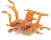
IPC 6013 breaks flex circuits out into four types: single layer (Type 1), double layer (Type 2), multi layer (Type 3), and rigid flex (Type 4).
Type 1 single-layer circuit.


Type 3 multi-layer circuit.

Types 1 and 2 circuits are generally very dynamic, meaning they can be exercised many times without performance-affecting damage. However, layer count isn’t the only determinant for how dynamic a circuit is. Layer thickness differences and materials specs can make two double-layer circuits as different as a Type 1 and Type 3.

Rigid-flex
Rigid-flex PCBs are a combination circuit, and they are expensive. Some applications, like double-sided surface mount, require the rigid-flex construct; however, the Minco engineers see a lot of unnecessary specs for rigid-flex. If the application calls for single-sided surface mount with flex, mounting a stiffener will do the job. It also will give you a 25–30% cost reduction from rigid-flex.

Stiffener used instead of rigid-flex.
Materials for the laminates of flex circuits include polyimide/acrylic — which dominates the North American flex market — LCP, and FEP. The copper in a flex circuit can be rolled annealed or electrodeposited, each with pros and cons.

No matter how small flex circuits’ slice of the overall circuit board market is, they can make or break a design. Spending some time familiarizing yourself with the terminology and methodology of flex can lead to better assemblies and smarter budgets, as well as deeper PCB fab relationships. One trade association meeting, or one class at a tradeshow conference, can pay exponential dividends.

Meredith Courtemanche, managing editor


*All images courtesy of Minco.

Monday, June 1, 2009

Adjusting to the Market: Merix Repositions for Mil/Aero Growth

It’s remarkable how some companies can adjust quickly to take advantage of a changing environment. In 2007, Merix Corp. (Beaverton, OR), saw an opportunity to expand from an under-diversified PCB manufacturer working mainly in networked communications to a company providing high-volume military and aerospace PCB manufacturing. Now, the company, which has been in operation for more than 40 years, has completed the transition to mil/aero PCB manufacturing house.

Michael Burger joined Merix as president and CEO in 2007, bringing with him the experience of many years with Flextronics. “We committed to a strategic realignment with a focus on expanding our technology and manufacturing capability to increase market share in the defense and aerospace sector,” said Burger. Now, the company has completed that phase, which Burger says will position it for long-term growth and profitability.

The military market has remained strong compared to the rest of the PCB market space. Nine percent of overall sales at Merix today come from military contractors, up from two percent in the past. One reason for the deluge in defense/aerospace business is that 16 new and potential clients have pushed the company to get qualifications going in the mil/aero space in just the last quarter. Merix San Jose is MIL-PRF-55110F certified and applying for MIL-PRF-31032 certification. Customer demands and increased business in this area have prompted growth in this market.

Read more about the transition to military/aerospace products in this news story: Merix Strengthens Defense and Aerospace Capability

Merix started as a board house for Tektronix more than 40 years ago. In 2004, the company expanded, buying Data Circuits, a quick-turn (10 days or less) operation in San Jose. Today, quick-turn prototyping of standard and advanced PCB technologies can be performed in 24 hours at Merix’s San Jose facility. A fully reconfigured 250,000-sq.ft. facility in Forest Grove, OR, also offers quick-turn prototyping to full-volume production, handling advanced technology options as high layer counts and high density interconnect (HDI) solutions. The company has always been a PCB manufacturer with a lot of prototyping business around communications (about 40% of sales) with the remainder in auto, computer and peripherals, medical and telecom.

Merix has two Asian facilities. A Huiyang, a 450,000-sq.ft. facility designated for high volume, low-mix PCB assembly and one in Huizhou, at 135,000 square feet. Approximately 40% of its business comes out of the North American customer base, starting out in quick-turn prototypes and then moving to high-volume production in the Asian facilities as designs prove robust enough for high-volumes. “Helping customers go from prototype in North America to volume production in Asia works well for us,” said Mike Zelman, VP of marketing.

Electronics manufacturing suppliers have to listen to what the market demands, relate to a variety of customer concerns, and keep in touch with technology trends to grow larger, no matter the market sector.

Gail Flower, editor-at-large